Multi-Scale Simulation of Reverse-Bias Breakdown in All-Perovskite Tandem Photovoltaic Modules under Partial Shading Conditions
Aeberhard, U., Natsch, N., Schneider, A., Zeder, S.J., Carrillo-Nuñez, H., Blülle, B. and Ruhstaller, B. (2024),
Sol. RRL 2400492.
https://doi.org/10.1002/solr.202400492
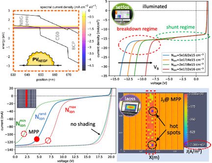
This research paper examines reverse-bias breakdown in all-perovskite tandem solar cells, particularly under partial shading conditions, and highlights how nonuniform active area quality, such as variations in mobile ion concentration, can impact their performance. The study uses a multi-scale simulation approach to demonstrate that an increase in mobile ion density significantly reduces the breakdown voltage and can lead to localized current hot spots in large-area modules. The authors suggest that these hot spots, caused by fluctuating mobile ion concentration, are potential degradation centers in the solar cells. They also suggest further investigation into factors like unintentional doping and additional breakdown mechanisms to better understand and improve the performance of these solar cells.
How SETFOS Was Used to Study Reverse-Bias Breakdown
The authors of the research paper use the device simulation tool SETFOS to perform cell-level simulations on all-perovskite tandem solar cells. Here's a breakdown of its role:
Drift-diffusion Simulation: SETFOS is used to simulate the behavior of charge carriers within the solar cell under a large reverse-bias voltage. This helps researchers visualize the band profile, or the energy levels of electrons within the device's various layers.
Mobile Ion Consideration: The simulations in SETFOS incorporate the effects of mobile ions within the perovskite layer, a crucial aspect that influences the breakdown voltage.
Coupling with Quantum Transport Simulation: The data from SETFOS, including the band profile and quasi-Fermi levels, are then used as input for a separate quantum transport simulation tool, PVnegf. This allows for a microscopic examination of the tunneling breakdown current.
Iterative Analysis: The tunnel generation rates, calculated in PVnegf, are fed back into SETFOS. This iterative process, with information exchanged between SETFOS and PVnegf, continues until the tunneling current converges, providing an accurate representation of the breakdown phenomenon.
Generating JV Curves: Through this coupled simulation approach, SETFOS ultimately helps generate current density-voltage (JV) curves for the all-perovskite tandem solar cell, even under reverse-bias conditions. These JV curves are essential for understanding how the device performs near its breakdown voltage.
In summary, SETFOS acts as the foundation for the cell-level simulations, providing crucial data about charge transport and mobile ion behavior, which is then combined with quantum transport calculations to comprehensively study reverse-bias breakdown in all-perovskite tandem solar cells.
Using Laoss to Simulate Large-Area Solar Module Behavior
The authors use Laoss, a large-area thin-film electronics modeling tool, to understand how the performance variations observed at the cell level translate to the behavior of a complete solar module12.
Here's a breakdown of its use:
●
Quasi-3D Module Simulation: Laoss enables a "2D+1D" simulation approach, treating the top and bottom electrodes with a 2D finite element method (FEM) while using a 1D coupling law to represent the vertical current flow through the active area of the solar cells within the module3.
●
Incorporating Cell-Level Data: The JV curves generated in SETFOS, which incorporate the effects of varying mobile ion densities and reverse-bias breakdown, are used as input for Laoss1. These curves act as the local 1D coupling law within the module simulation, linking the 2D electrode simulations3.
●
Module Design and Interconnection: The researchers incorporate design parameters of a real all-perovskite tandem module into the Laoss simulation. These parameters, taken from a previously calibrated model4, include sheet resistances of electrodes, scribe line geometries for monolithic interconnection, and the Ohmic properties of the P2 scribe2.
●
Spatial Resolution: Laoss simulates a 10 cm x 10 cm module with a spatial resolution of 3 x 30 pixels per cell stripe, totaling 900 pixels. Each pixel is randomly assigned a JV curve based on a Gaussian distribution of mobile ion concentrations, representing real-world variations in manufacturing2.
●
Partial Shading Analysis: The study simulates both full and partial shading conditions on a single cell stripe within the module using Laoss5. This allows the authors to observe how variations in mobile ion density (and thus, breakdown voltage) at the pixel level affect current flow and hot spot formation under these conditions6.
In essence, Laoss allows the researchers to scale up their analysis from the behavior of individual solar cells to a complete module, taking into account the realistic variations in properties and the effects of partial shading. This multi-scale approach, linking the detailed device physics simulated in SETFOS to the module-level performance predicted by Laoss, provides a powerful tool for understanding and mitigating potential degradation mechanisms in all-perovskite tandem solar cells.

Investigating the electrical crosstalk effect between pixels in high‑resolution organic light‑emitting diode microdisplays
Kang, H., Hwang, Y., Kang, Cm. et al.
Sci Rep 13, 14070 (2023).
https://doi.org/10.1038/s41598-023-41033-4
This research explores electrical crosstalk in high-resolution OLED microdisplays impacting color distortion, especially in AR/VR applications. Through simulations and experimental measures, it was found that decreasing sheet resistance in the common organic layer elevated crosstalk, and increasing pixel density led to a color gamut reduction.
How Laoss Simulation was used
Simulation process. Commercial software LAOSS (Fluxim) which used 2 + 1D finite element model based on the conductivity of the common layer17,18 and J–V–L characteristics of the fabricated white OLED were used for the electrical crosstalk calculation.

Deep ensemble inverse model for image-based estimation of solar cell parameters
M. Battaglia, E. Comi, T. Stadelmann, R. Hiestand, B. Ruhstaller, E. Knapp;
APL Mach. Learn. 1 September 2023; 1 (3): 036108.
https://doi.org/10.1063/5.0139707
A data-driven approach using deep learning predicts parameters of a solar cell model based on electroluminescence (EL) images. Using 75,000 synthetic EL images, the study employs a deep ensemble of 17 modified VGG19 neural networks to add uncertainty estimates. This approach, tested on four solar cell samples, bridges deep learning with engineering applications needing real-time physical model parameterizations with confidence intervals. The network's predictions showed an average deviation of 0.2% (max 10%) in junction voltage values, confirming the method's validity.
How Laoss was Used
Laoss, a simulation model, was used to model the measured solar cell samples and generate simulated electroluminescence (EL) images. These images were then used to train the inverse convolutional neural network (CNN) model. The Laoss parameterization used to generate the training data is discussed in the paper. The inverse model was trained on a set of simulated EL images, and the network architecture and training of the inverse CNN model are explained in detail. The results of the inverse model method are evaluated, and the changes in the CNN structure and training hyperparameters required to implement and train such a deep ensemble CNN inverse model are discussed.

A touchless user interface based on a near-infrared-sensitive transparent optical imager
Kamijo, T., van Breemen, A.J.J.M., Ma, X. et al. A touchless user interface based on a near-infrared-sensitive transparent optical imager. Nat Electron (2023).
https://doi.org/10.1038/s41928-023-00970-8
Researchers have developed a touchless user interface based on a visually transparent near-infrared-sensitive organic photodetector (OPD) array. The touchless interface can be used on top of a display, eliminating the need for physical contact.
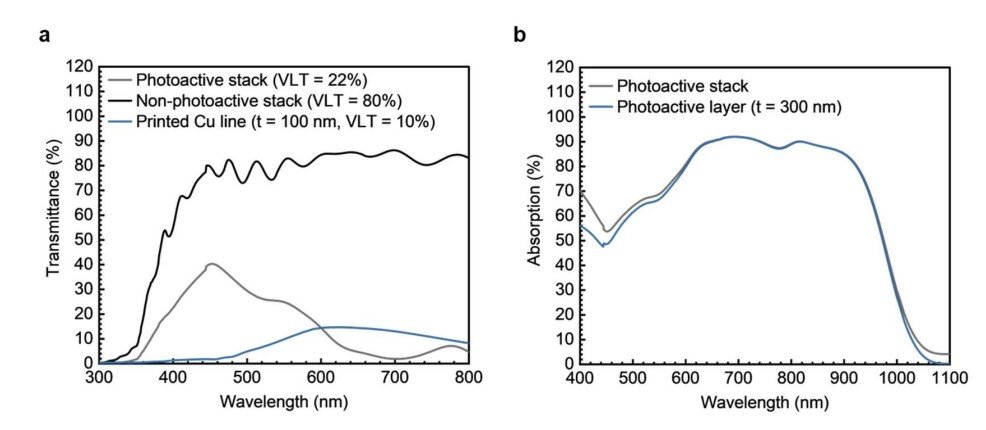
The OPD array is designed with optical transparency in mind, using printed copper grids and patterned organic photodetector subpixels. The design optimization results in a high photodetectivity of 10^12 Jones at 850 nm and a visible-light transmittance of 70%.
The touchless user interface can be used with a penlight or through gesture recognition, providing a hygienic and convenient alternative to traditional touch screens. The technology has potential applications in automated teller machines (ATMs), ticket vending machines, and kiosks, where hygiene is a concern. It is a scalable and flexible solution that can be integrated into a variety of display applications without size limitations or calibration requirements. 2D FEM simulations for the surface potential and the current density distributions derived from the printed Cu grid structure .
How Fluxim’s Research Tools were used
Setfos
Numerical electro-optical simulations for the photogenerated J–V curves of our NIR-sensitive OPDs were performed by using Setfos.
The VLT of the parallel OPD subpixel array was calculated by the summation of the simulated optical transmittance for each component using Setfos
Laoss
2D FEM simulations for the surface potential and the current density distributions derived from the printed Cu grid structure for our NIR-sensitive OPDs were performed by Laoss 4.0

Color gamut change by optical crosstalk in high-resolution organic light-emitting diode microdisplays
Soobin Sim, Jinha Ryu, Dae Hyun Ahn, Hyunsu Cho, Chan-mo Kang, Jin-Wook Shin, Chul Woong Joo, Gi Heon Kim, Chun-Won Byun, Nam Sung Cho, Hyoc Min Youn, Young Jae An, Jin Sun Kim, Hanyung Jung, and Hyunkoo Lee,
Opt. Express 30, 24155-24165 (2022)
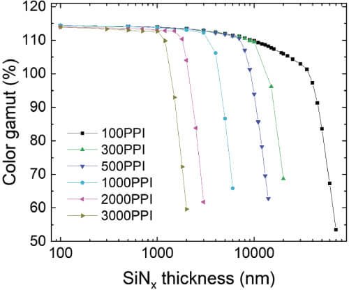
Herein, the color gamut change by optical crosstalk between sub-pixels in high-resolution full-color organic light-emitting diode (OLED) microdisplays was numerically investigated. The color gamut of the OLED microdisplay decreased dramatically as the pixel density of the panel increased from 100 pixels per inch (PPI) to 3000 PPI.
Both Setfos and Laoss were used by the research team to perform optical simulations. To conduct the optical crosstalk simulation, the EL spectra was simulated using Setfos and the simulated EL spectra were well matched with the measured EL spectra. The transmittances of the R and G CFs provided by Laoss.

Scaling Considerations for Organic Photovoltaics for Indoor Applications
Gregory Burwell, Oskar J. Sandberg, Wei Li, Paul Meredith, Matt Carnie, and Ardalan Armin
Sol. RRL 2200315, 1 , (2022)
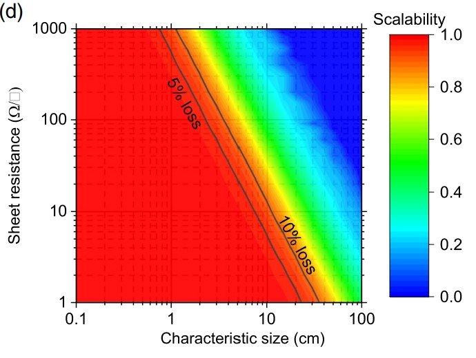
Compared to their use as organic solar cells (OSCs) for standard outdoor solar harvesting, indoor OPV (IOPV) devices operate at low light intensities and thus demonstrate different area-scaling behavior. In particular, it appears as though the performance of large-area IOPV devices is much less affected by the sheet resistances of the transparent conductive electrodes (a major limit in OSCs), but instead by factors such as their shunt resistance at low light intensities. Herein, the key parameters for improving the efficiency of large area IOPV using drift-diffusion and finite element modeling (FEM) are examined. The scaling behavior at low-light intensities is theoretically and experimentally probed and demonstrated using the model PM6:Y6 system.

Printed Copper Grid Transparent Conducting Electrodes for Organic Light-Emitting Diodes
Takeshi Kamijo, Suzanne de Winter, Pradeep Panditha, and Eric Meulenkamp
ACS Applied Electronic Materials 2022 4 (2), 698-706
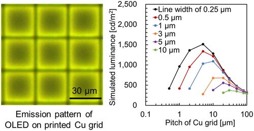
The transparent conductive electrode (TCE) is a key component of organic light-emitting diodes (OLEDs). High resolution printed metal grids are a promising alternative to indium tin oxide (ITO). We present results for evaporated OLEDs with a printed copper (Cu) grid with line width below 3 μm. The use of a thick doped hole injection layer (HIL) prevented electrical shorts and resulted in good quality OLEDs with acceptable leakage current. We report a detailed analysis of the microscopic uniformity of light emission and compare the measured data with simulations based on finite element modeling (FEM) to investigate various factors that contribute to differences between the Cu grid OLED and ITO reference device. This insight resulted in design rules that enable a luminance of the Cu grid OLED that can potentially equal that of an ITO-based equivalent OLED by using a very fine pitch and narrow line width of 5 μm and 250 nm, respectively, within the capabilities of state-of-the-art printing technology.
The spatial luminance distribution was simulated by LAOSS - large area organic semiconductor simulation software.

Sinusoidal small-signal (AC) and steady-state (DC) analysis of large-area solar cells
Ennio Luigi Comi,Evelyne Knapp, Stefano Weidmann, Christoph Kirsch, Sandra Jenatsch, Roman Hiestand, Beat Ruhstaller
Solar Energy Advances
Volume 1, 2021, 100003
doi.org/10.1016/j.seja.2021.100003
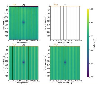
In this paper the researchers present a FEM (Finite Element Method) software that supports the upscaling process from small to large area solar cells and tackles the efficiency loss factors of scaling solar cells such as shunts and increasing series resistance caused by the sheet resistance of the electrodes.

An underestimated photoactive area in organic solar cells based on a ZnO interlayer
Z. Chen, J. Wang, H. Jin, J. Yang, Q. Bao, Z. Ma, W. Tress and Z. Tang
J. Mater. Chem. C (2021)
https://pubs.rsc.org/en/content/articlelanding/2021/tc/d1tc00745a
The authors studied the impact of the resistance of a sol-gel-grown ZnO interlayer on the efficiency of an organic solar cell. They find that the UV-induced doping effect leads to a significantly reduced ZnO resistance, which gives rise to an underestimated photoactive area and thus overestimated short-circuit current density (Jsc) Therefore, the validity of the argument that high-resistance interlayers do not lead to overestimated Jsc should always be carefully evaluated. Current-voltage characteristics were simulated using the large-area semiconductor simulator LAOSS

Parameterization of Metallic Grids on Transparent Conductive Electrodes for the Scaling of Organic Solar Cells
G. Burwell, N. Burridge, E. Bond, W. Li, P. Meredith, and A. Armin
Adv. Electron. Mater. (2021), 2100192,
https://onlinelibrary.wiley.com/doi/10.1002/aelm.202100192
Finite element modeling is used to investigate the relevant design parameters and to estimate figures of merit for realistic large-area OPVs. It is shown that the scalability of devices with metallic grids improves significantly when grids are implemented at micrometer scales. Representative silver grids are fabricated and the optical and electrical properties of the resulting structures are measured. These findings indicate that metallic grids can be designed to develop large-area solution-processed solar cells with currently available fabrication techniques.

Perovskite Solar Modules: Design Optimization
Diogo Castro, Vera C. M. Duarte, and Luísa Andrade
ACS Omega Article ASAP
The increasing demand for solar energy has led researchers worldwide to develop new photovoltaic technologies.
Among these, perovskite materials are one of the most promising candidates, with a performance evolution unparalleled in the photovoltaic field.
However, this thin-film technology is not yet available at a commercial level, mainly due to upscaling issues. This work studied the best design options for upscaling single cells into modules by minimizing electrical losses in the device substrates.
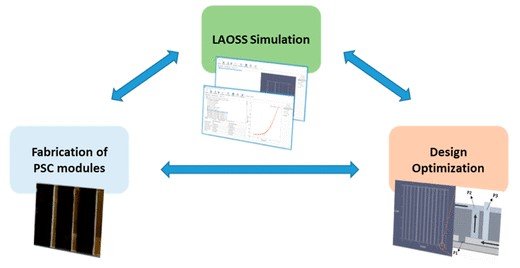
Fluxim`s Laoss software for upscaling was used to test and optimize different substrate sizes and designs and to predict several performance outcomes from experimentally fabricated single cells.
The results showed that it is possible to retain most of the energy production when upscaling from a single cell to a module if the appropriate design for an efficient monolithic device is used.
