How to correctly simulate the EQE of an organic tandem solar cell using full optoelectronic simulations
When selecting a PV technology, both efficiency and durability play a vital role, especially since installation costs can make up a large share of the total investment. Single junction solar cells, though widely used, are limited in their ability to convert sunlight into energy efficiently. This has led to interest in tandem solar cells, which can harness a broader range of the solar spectrum and potentially improve energy output.
However, the added complexity of tandem cells introduces challenges like higher fabrication costs in four-terminal designs or the need to match current and ensure long-term stability in two-terminal configurations. These drawbacks can offset the benefits of tandem solar cells if not properly addressed.
In this blog post, we’ll take a closer look at a well-known organic tandem cell from the literature, and we will show how our simulation software SETFOS can help pinpoint and address design limitations in this tandem OPVs.
Cell architecture
The modeled organic tandem solar cell consists of a top cell with DR3TSBDT:PC71BM as absorbing layer and a bottom cell with DPPEZnP-TBO:PC61BM as absorber, as described by Li et al. [1] The two sub-cells are connected by a recombination interlayer composed of ZnO and PEDOT:PSS. CuSCN and PFN are used as thin electron and hole blocking layers at the anode and cathode site. ITO and Al form the electrodes. The layer stack is shown in Figure 1..
Setup the opto-electronical model
A coupled optoelectrical simulation in SETFOS can be split into two parts: an optical simulation and the electrical simulation. The optical simulation is required to understand the maximum possible absorptance and EQE achievable with the solar cell. For an optical simulation, Setfos uses a 1D-model based on transfer matrix and net radiation methods for both coherent and incoherent light propagation. On the other hand, the combined optoelectronic simulation shows the effect of various losses in each layer of the stack.
In the electrical part of the coupled optoelectrical simulation solves the continuity equation in 1D together with the drift-diffusion current coupled to the Poisson equation for the electrostatic potential. To describe the charge transfer at the interface between the two sub-cells, we use the hopping model based on the Miller-Abrahams (MA) theory. This model is also implemented in SETFOS and describes thermally activated hopping in disordered materials.
To start the opto-electronical simulation, input parameters for both the optical and electrical simulations are required. To perform the optical simulation, the refractive index data (nk) are used as material parameters. These can be obtained through ellipsometry measurements or sourced from literature, as in our case. [2, 3] For the electrical simulation, the HOMO and LUMO energy levels of all materials in the stack are required.In general, these can be obtained, for example, from the oxidation potential measured via cyclovoltammetry, from the optical band gap , or through quantum chemical calculations, such as TDDFT. Figure 1 shows the layer stack including the respective energy levels and wavelength dependent nk-values for DR3TSBDT:PC71BM and DPPEZnP-TBO:PC61BM. [1, 2, 3]

Figure 1: Simulation setup for the optical and electronical part of the coupled simulation.
Additional input parameters for the electronic simulation are the field-dependent charge carrier mobilities and the recombination rate. We extracted them by using a global multi-parameter optimization routine to match the experimental single junction and tandem device characteristics reported in Li et al. [1] In our example, all parameters were validated for accuracy by comparing both the single junction and tandem device results (Figure 2).
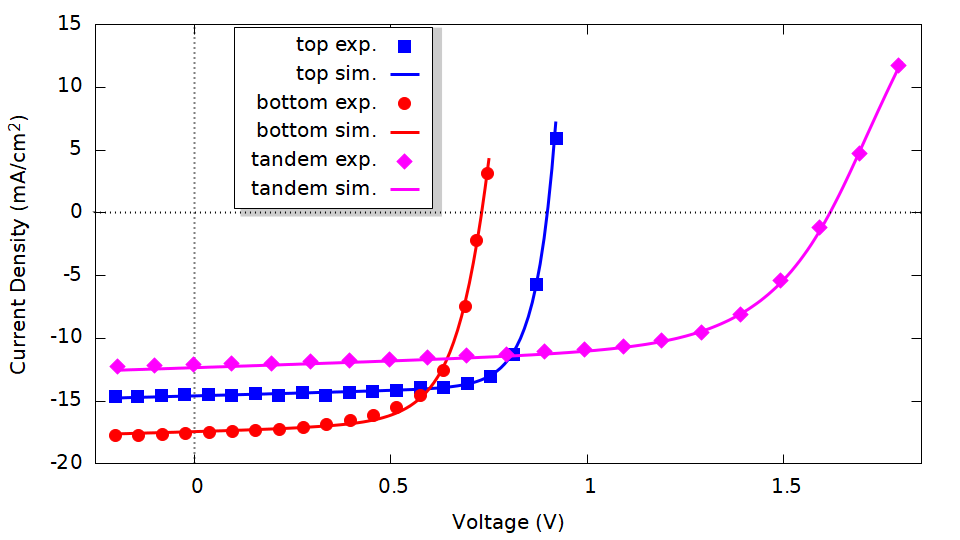
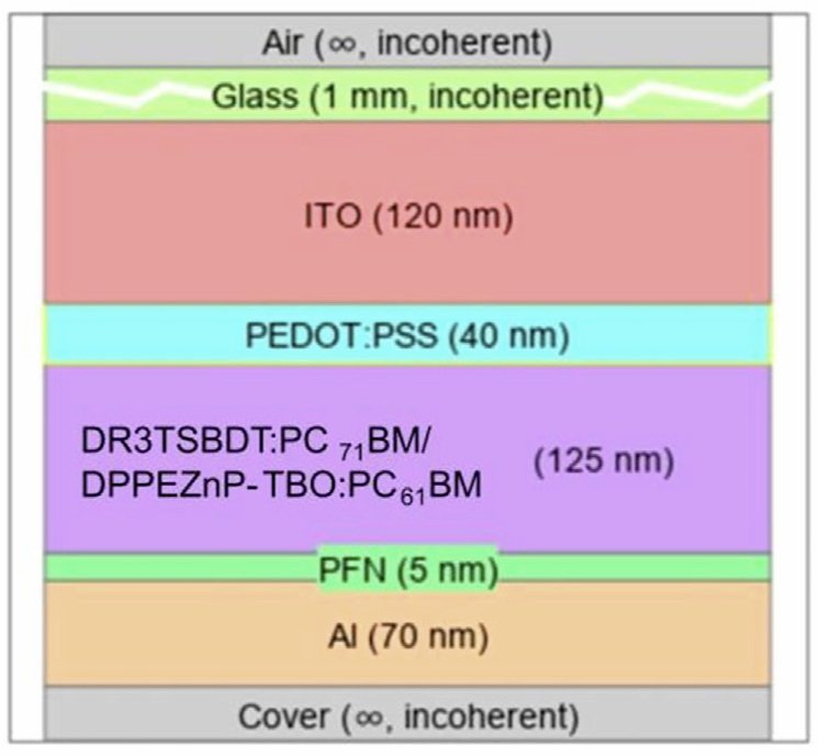
Figure 2: Experimental and simulated JV characteristics of the single junction sub-cells and tandem cell described in the text (left). On the right is the single junction layer stack implemented in Setfos.
Analysis of Single Junction and Tandem Characteristics with focus on the EQE simulation
Now that the model is validated, we can identify and analyze electrical losses in the tandem OPV and to compare the external quantum efficiency (EQE) with the absorptance.
Accurately determining the EQE of organic tandem devices is challenging because, to probe a specific sub-cell, this cell must be the device that is limiting the current across the entire wavelength range. Creating this condition requires appropriate bias illumination. An additional challenge with OPVs is that the carrier extraction efficiency depends strongly on the built-in field, which, in turn, changes with illumination. To solve this, we first establish in the simulation the same conditions that are found under AM1.5G illumination at global short circuit conditions (Jₛ꜀
). This is done by applying an additional bias voltage in the simulation.
The model setup enables the simulation of the current flow through the entire solar cell, allowing us to closely replicate the experimental setting. This means that we can use monochromatic bias light with an intensity adjusted to approach AM1.5G illumination. A view to the wavelength dependent extinction coefficients (Figure 3) shows the best monochromatic illumination wavelength, to establish those conditions for the top and bottom cell i.e 470 nm and 700 nm. In other words, to measure the top-cell EQE, we bias the bottom cell with 700 nm and vice versa. Then, we obtain the EQE in differential form from the additional current induced by the weak monochromatic probe beam.
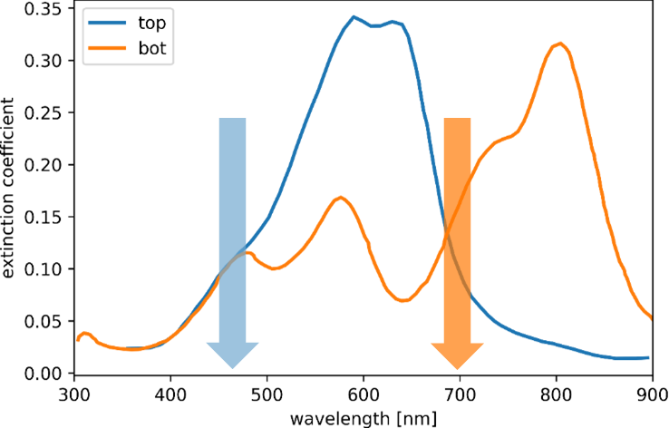
Figure 3: Bias illumination applied for the determination of the EQE in tandem configuration. Shown here is the sub-cell extinction coefficient and spectral location of the monochromatic bias light.
Figure 4 shows the simulated EQE for the two sub-cells and the tandem OPV. The dashed line shows the EQE under bias light only and the solid line with an additional voltage bias. The EQE can be compared with the experimental data for the same solar cell, as reported in the literature [1]. The comparison of the simulation and the measured EQE shows good qualitative agreement.
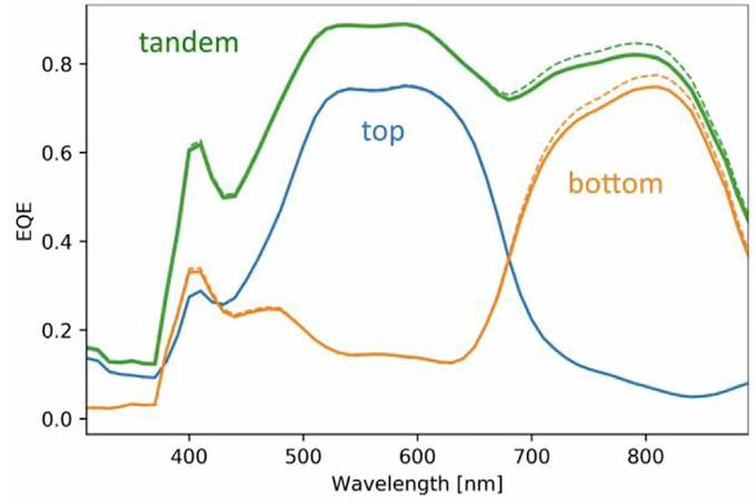
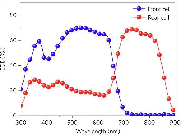
Figure 4: (Left) Sub cell EQE from coupled simulation under application of bias light only (dashed lines) and with additional bias voltage (solid lines). Right) measured EQE from Li et al. [1]
Now, we can ensure the internal consistency of the procedure by comparing the simulated current density at short-circuit Jₛ꜀ under AM1.5G with the value obtained by integrating the product of EQE and AM1.5G flux over the specific wavelength.
Under the AM1.5G spectrum it becomes visible that the performance of this tandem device is limited by the top cell. Therefore, we consider the current density extracted from the EQE of the top sub-cell, i.e. 12.19 mA/cm² for AM1.5G illumination and 12.22 mA/cm² for the 700 nm bias light at 0 V.
The small disagreement is a consequence of the larger reverse top-cell voltage under the 700 nm bias light (Vtop= 0.88 V) versus (Vtop = 0.53 V) under AM1.5G illumination. The difference can be corrected by the application of a corresponding forward bias voltage (V = 0.35 V), for which the exact short circuit current density can be recovered. The resulting current density under 700 nm bias light is then 12.19 mA/cm² (see Figure 5).
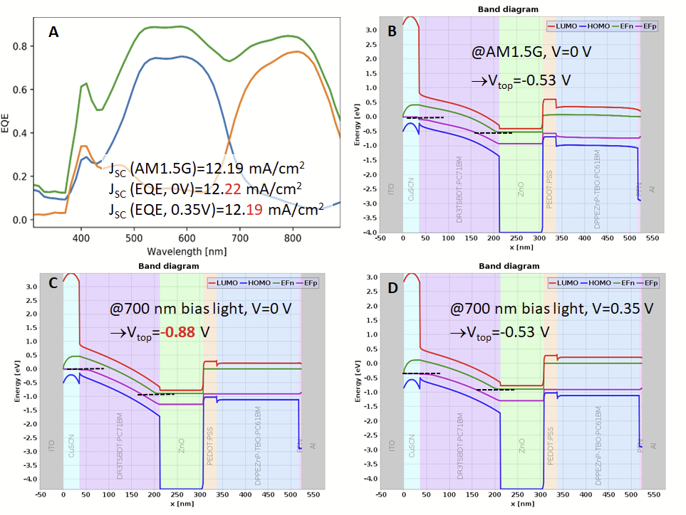
Figure 5: A shows the sub-cell EQE from coupled simulations under the application of bias light only (dashed lines) and with additional bias voltage (solid lines). B shows the band profile and quasi-Fermi level at short circuit conditions (V = 0V) and under illumination with the AM1.5G spectrum, for which a top-cell voltage of V=0.53 V develops. C shows the band profile and quasi-Fermi level under 700 nm bias light, the top-cell voltage at short circuit conditions amounts to V=0.88V. In D, the application of a bias voltage of V=0.35 V reproduces the AM1.5G short circuit conditions under bias light.
Now, it is possible to compare the EQE to the absorptance. Figure 6 shows the simulated layer-resolved absorptance of the tandem OPV including the recombination junction (yellow line, coupled) and of the individual optically filtered sub-cells (white line, non-coupled). Parasitic contributions are displayed in red. The contributions of the top and bottom sub-cells are indicated with dashed and dotted lines, respectively. The comparison reveals that the non-coupled simulation underestimates the charge extraction efficiency at short circuit conditions.
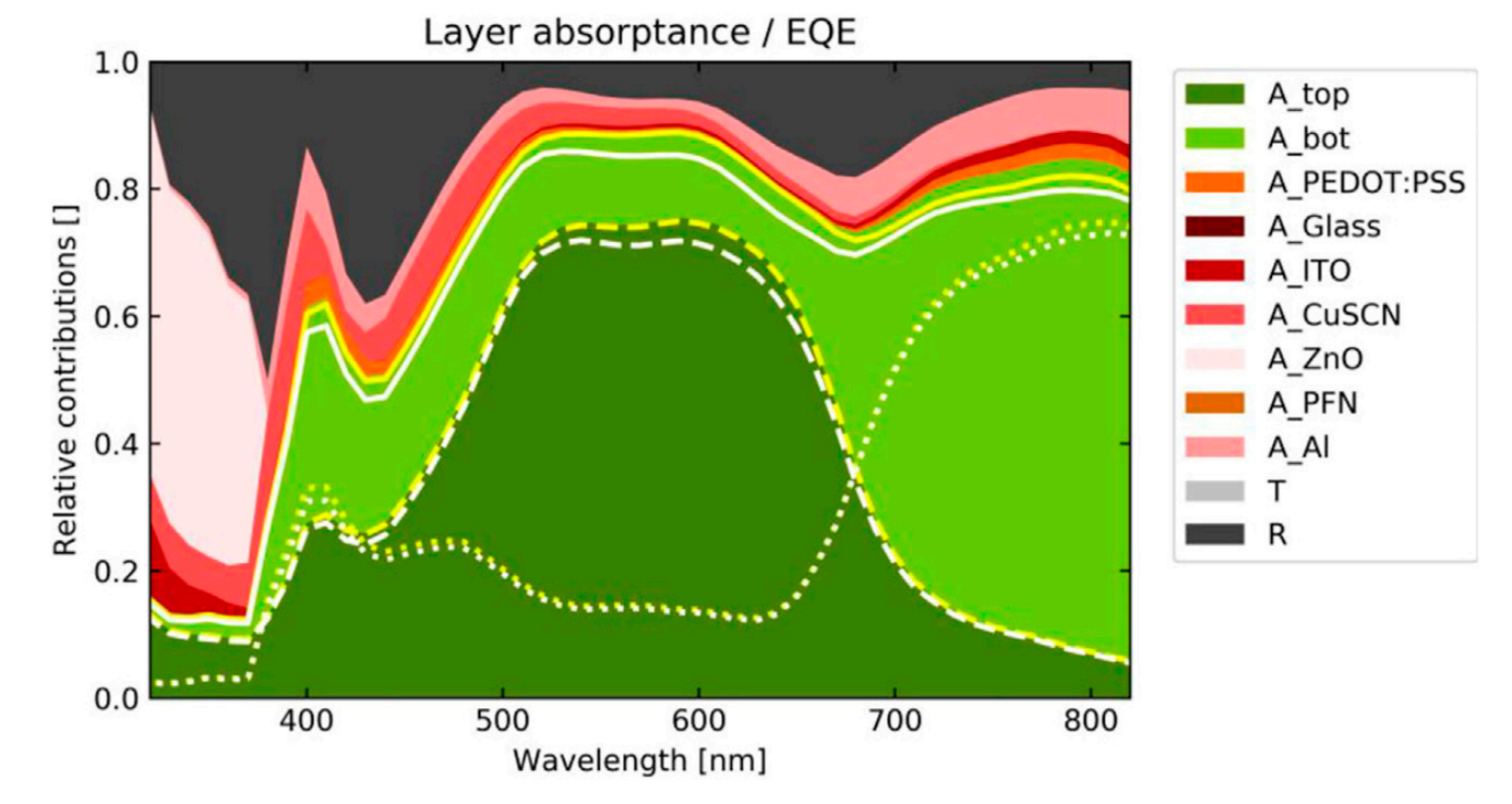
Figure 6: Layer resolved absorptance and EQE as obtained from the coupled and noncoupled electronical simulations. The contributions of the top and bottom sub-cells are indicated with dashed and dotted lines and the parasitic contributions are shown in red.
This is a summary of our work on tandem OPVs. If you found this topic interesting, Dr. Urs Aeberhard from our R&D team shows further analysis in his paper: Aeberhard, U. et al. Analysis and Optimization of Organic Tandem Solar Cells by Full Opto-Electronic Simulation. Front. Photon. 3, 891565 (2022).
The paper further addresses:
The impact of electronical non- idealities on the tandem characteristics.
The impact on the JSC and EQE to the charge transfer rate at the recombination junction.
The impact of the charge carrier hopping rate at the recombination junction on the JV characteristics.
All simulations have been performed with the simulation software SETFOS.
References:
[1] Li, M. et al., 2017, Nature Photon. 11, 85.
[2] Kumari, T., et al., 2017, Energy Environ. Sci., 10, 258.
[3] Xiao, L., et al., 2017, ACS Appl. Mat. Interfaces, 9, 29917.


