Advanced Optical Simulation to Develop Curved OLED and LCD Displays
Curved and flexible displays have risen in popularity in recent years and will continue to do so with high demand coming from several sectors.
This is most visible, of course, in smartphones and tablets, where there is a constant need for innovation in order to keep consumer interest. Further demand is also emerging at a rapid pace from the automotive and lighting sectors. Thus R&D into next-generation displays remains strong.
All of these applications require dedicated features for the control of light-guiding and outcoupling due to the curved geometry. However, most microtextures for beam shaping are designed for flat devices, and their appropriateness for curved geometries needs to be evaluated.
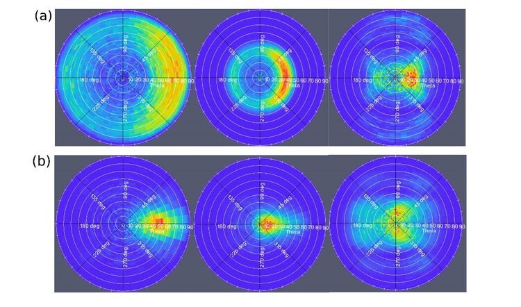
In this post, we demonstrate, through the use of simulation, the impact of curved geometries on beam shaping and control of light outcoupling via microtextures in backlight units for LCD displays.
📹 Laoss Optics Tutorial
Simulation of curved backlight displays with Laoss Optics
In this video tutorial, Dr. Urs Aeberhard demonstrates how to use the Optics module of Laoss to rapidly model a curved display backlight unit. Urs is using Fluxim’s 3D ray-tracing tool Laoss Optics to determine the impact of curved geometries on beam shaping. He is also demonstrating how to design suitable structures to control light outcoupling via microtextures in backlight units for LCD displays.
If you want to test Laoss we will send you a free evaluation license.
📜Simulation of Beam Shaping by Micro-textures for Curved Displays
Urs Aeberhard, Roman Hiestand, and Beat Ruhstaller
In this paper, which was first presented at the SID 2021 conference, we demonstrated how to simulate the guiding and out-coupling of light in strongly curved backlight units with edge illumination using a 3D ray-tracing tool with custom light emission and scattering features. The impact of the display curvature is assessed regarding the uniformity and angular characteristics of light outcoupling in a complex backlight with position-dependent bottom roughness, a diffuser element, and a textured brightness enhancement film.
An essential component of LCDs is the backlight units (BLU), which provide uniform white illumination to the LCD pixel array. In order to achieve the required level of spatial and angular uniformity as well as luminance, modeling of the BLU is an instrumental element in the BLU design process but, in general, represents a major challenge. In the case of flexible, thin, and lightweight applications, an edge-lit configuration (indirect illumination) is often favored, where the light needs to be scattered as a function of distance from the source, and light extraction is at an angle normal to injection. Ray-tracing simulations were shown to be useful for the design of various beam shaping features for optimized light-guide plate design. However, the beam shaping features were optimized for flat display applications. As this might no longer be ideal for non-flat light guide plates, we investigate the simulation of backlights in bent geometries for use with curved LCDs.
📃Read the full paper here
Get Laoss FREE for 1-Month and Try it Out
📈How to Reduce Efficiency Loss When Scaling up Your Device
Have you tried to scale up your Organic Light-Emitting Diode to large areas just to discover that the efficiency was considerably lower than the lab-scale device?
For both LEDs and solar cells, the scaling-up process is a challenge, also because of the high sheet resistance of the transparent electrode (TCE). The TCE needs to be thin enough to be optically transparent, but not a high resistivity element that hinders the charge injection/extraction.
An optimized electrode with low sheet resistance and high transmittance can be designed with the simulation software LAOSS.
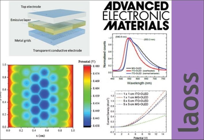
Researchers at Swansea University exploited FEM simulation to compare OLEDs with a thin-film TCE and with a transparent metal grid added to the TCE. The reduced potential drop from the presence of grids is shown to lower the Joule heating at the TCE, resulting in higher power conversion efficiency and luminosity, as well as improved device stability. The proposed strategy could enable the fabrication of large-area OLED for lighting with reduced resistive losses and lower usage of indium with respect to the current fabrication methods.
Access The Paper Here
🆕Laoss (Large-Area Organic Semiconductor Simulation) 4.1 - What’s New?
If you’re an existing Loass user or simply considering the benefits of using simulation to upscale your device then you’ll be interested in the latest release of the software, version 4.1.1.
In addition to the functions detailed in the image below we’ve now added:
Movable detector can produce wavelength-dependent and color output
Improved scaling in plots of geometries
XY plots are now shown in the same units as interface-geometries
Laoss-Setfos Integration with Setfos 5.1
⭐Here’s what researchers are saying about Laoss
We have extensively used both SETOS and LAOSS in our recent endeavour to model large-area OPV and OLED devices. The intuitive workflow of both software packages allows us to quickly try out new ideas before realising them experimentally.“
Dr. Ardalan Armin, Ser-SAM group, Department of physics, Swansea University
⏩ Evaluate Your Scaled Device in Seconds Not Hours
Using simulation to scale your device can measurably save hours of trial and error experimentation and decrease your time to publish/market. We appreciate that advanced simulation software can often involve a steep learning curve and time is often not on your side. To that end, we’d be happy to support your learning experience and share our expertise in how to get the most out of Laoss.


